-
MIT, Applied Materials and the Northeast Microelectronics Coalition Hub to Bring 200mm Advanced Research Capabilities to MIT.nano
Source: Nasdaq GlobeNewswire / 30 Jan 2024 12:13:54 America/Chicago
CAMBRIDGE, Mass. and SANTA CLARA, Calif., Jan. 30, 2024 (GLOBE NEWSWIRE) -- MIT and Applied Materials, Inc. announced an agreement today that, together with a grant to MIT from the Northeast Microelectronics Coalition (NEMC) Hub, commits more than $40 million of estimated private and public investment to add advanced nano-fabrication equipment and capabilities to MIT.nano, the Institute’s center for nanoscale science and engineering. The collaboration will create a unique open-access site in the United States that supports research and development at industry-compatible scale using the same equipment found in high-volume production fabs to accelerate advances in silicon and compound semiconductors, power electronics, optical computing, analog devices and other critical technologies.
The equipment and related funding and in-kind support provided by Applied Materials will significantly enhance MIT.nano’s existing capabilities to fabricate up to 200mm (8-inch) wafers, a size essential to industry prototyping and production of semiconductors used in a broad range of markets including consumer electronics, automotive, industrial automation, clean energy and more. Positioned to fill the gap between academic experimentation and commercialization, the equipment will help establish a bridge connecting early-stage innovation to industry pathways to the marketplace.
“A brilliant new concept for a chip won’t have impact in the world unless companies can make millions of copies of it. MIT.nano’s collaboration with Applied Materials will create a critical open-access capacity to help innovations travel from lab bench to industry foundries for manufacturing,” said Maria Zuber, MIT’s Vice President for Research and E. A. Griswold Professor of Geophysics. “I am grateful to Applied Materials for its investment in this vision. The impact of the new toolset will ripple across MIT and throughout Massachusetts, the region, and the nation.”
Applied Materials is the world’s largest supplier of equipment for manufacturing semiconductors, displays and other advanced electronics. The company will provide at MIT.nano several state-of-the-art process tools capable of supporting 150 and 200mm wafers and will enhance and upgrade an existing tool owned by MIT. In addition to assisting MIT.nano in the day-to-day operation and maintenance of the equipment, Applied engineers will develop new process capabilities which will benefit researchers and students from MIT and beyond.
“Chips are becoming increasingly complex, and there is tremendous need for continued advancements in 200mm devices, particularly compound semiconductors like silicon carbide and gallium nitride,” said Aninda Moitra, Corporate Vice President and General Manager of Applied Materials’ ICAPS Business. “Applied is excited to team with MIT.nano to create a unique, open-access site in the U.S. where the chip ecosystem can collaborate to accelerate innovation. Our engagement with MIT expands Applied’s university innovation network and furthers our efforts to reduce the time and cost of commercializing new technologies while strengthening the pipeline of future semiconductor industry talent.”
The Northeast Microelectronics Coalition (NEMC) Hub, managed by the Massachusetts Technology Collaborative (MassTech), will allocate $7.7 million to enable the installation of the tools. The NEMC is the regional “hub” that connects and amplifies the capabilities of diverse organizations from across New England plus New Jersey and New York. The U.S. Department of Defense (DoD) selected the NEMC Hub as one of eight Microelectronics Commons Hubs and awarded funding from the CHIPS and Science Act to accelerate the transition of critical microelectronics technologies from lab-to-fab, spur new jobs, expand workforce training opportunities and invest in the region’s advanced manufacturing and technology sectors.
The Microelectronics Commons program is managed at the federal level by the Office of the Under Secretary of Defense for Research and Engineering (OUSD(R&E)) and the Naval Surface Warfare Center, Crane Division, and facilitated through the National Security Technology Accelerator (NSTXL), which organizes the execution of the eight regional hubs located across the country. The announcement of the public sector support for the project was made at an event attended by leaders from the DoD and NSTXL during a site visit to meet with NEMC Hub members.
“The installation and operation of these tools at MIT.nano will have a direct impact on the members of the NEMC Hub, the Massachusetts and Northeast regional economy, and national security. This is what the CHIPS and Science Act is all about,” said Ben Linville-Engler, Deputy Director at the MassTech Collaborative and the interim director of the NEMC Hub. “This is an essential investment by the NEMC Hub to meet the mission of the Microelectronics Commons.”
MIT.nano is a 200,000 square-foot facility located in the heart of the MIT campus with pristine, class-100 cleanrooms capable of accepting these advanced tools. Its open-access model means that MIT.nano’s toolsets and laboratories are available not only to the campus but also to early-stage R&D by researchers from other academic institutions, non-profit organizations, government and companies ranging from Fortune 500 multinationals to local startups. Vladimir Bulović, faculty director of MIT.nano, said he expects the new equipment to come online in early 2025.
“With vital funding for installation from NEMC and after a thorough and productive planning process with Applied Materials, MIT.nano is ready to install this toolset and integrate it into our expansive capabilities that serve over 1,100 researchers from academia, startups, and established companies,” said Bulović, who is also the Fariborz Maseeh Professor of Emerging Technologies in MIT’s Department of Electrical Engineering and Computer Science (EECS). “We’re eager to add these powerful new capabilities and excited for the new ideas, collaborations, and innovations that will follow.”
As part of its arrangement with MIT.nano, Applied Materials will join the MIT.nano Consortium, an industry program comprising 12 companies from different industries around the world. With the contributions of the company’s technical staff, Applied Materials will also have the opportunity to engage with MIT’s intellectual centers, including continued membership with the Microsystems Technology Laboratories (MTL).
About Applied Materials
Applied Materials, Inc. (Nasdaq: AMAT) is the leader in materials engineering solutions used to produce virtually every new chip and advanced display in the world. Our expertise in modifying materials at atomic levels and on an industrial scale enables customers to transform possibilities into reality. At Applied Materials, our innovations make possible a better future. Learn more at www.appliedmaterials.com.About MIT.nano
MIT.nano is an advanced facility for nanoscience and nanoengineering at the Massachusetts Institute of Technology. Located in the heart of the MIT campus, the facility provides shared equipment, specialized environments, and support from highly qualified technical staff to any faculty member, researcher, student, or qualified partner who needs these resources to advance their investigations.Researchers from MIT constitute the primary user community; individuals from other academic institutions, industry collaborators, member companies in the MIT.nano Consortium, and other external organizations may also access MIT.nano. Sharing resources through MIT.nano enables the MIT community to acquire the state-of-the-art equipment that would be challenging for individual labs or departments to afford or maintain on their own. The ample size of the 200,000-square-foot research facility also allows MIT to look beyond the present state-of-the-art by seeding dedicated lab spaces where new nanoscience and nanotechnology tools, instruments, processes, and techniques can be reinvented.
For more information, visit mitnano.mit.edu.
About the NEMC Hub
The mission of the Northeast Microelectronics Coalition (NEMC) Hub is to create a vibrant, well-connected ecosystem that meets the needs of the U.S. Department of Defense (DOD), while fostering genuine engagement across the region to provide sustainable lab-to-fab enablement and strengthen the domestic microelectronics workforce. With the Massachusetts Technology Collaborative (MassTech) as the Hub Lead, the NEMC Hub consists of more than 160 member organizations from industry, academia, and government representing unique mix of defense-oriented microelectronics organizations with world-leading technical expertise, facilities, resources, and infrastructure. The NEMC Hub is poised to deliver on the mission of the national Microelectronics Commons network, helping stimulating job creation, startup maturation, workforce training opportunities, and investments in the region’s advanced manufacturing and emerging technology sectors.Contact:
Ricky Gradwohl (editorial/media) 408.235.4676
Michael Sullivan (financial community) 408.986.7977A photo accompanying this announcement is available at https://www.globenewswire.com/NewsRoom/AttachmentNg/b8d41999-ade8-491c-8e2f-55f0abbb4823

Applied Materials Producer® CVD 200mm System
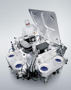
As part of the agreement announced today, Applied Materials will provide MIT.nano with several state-of-the-art 150mm and 200mm wafer processing systems, such as this Producer® chemical vapor deposition (CVD) system. The collaboration will create a unique open-access site in the United States that supports research and development at industry-compatible scale to accelerate advances in silicon and compound semiconductors, power electronics, optical computing, analog devices and other critical technologies.